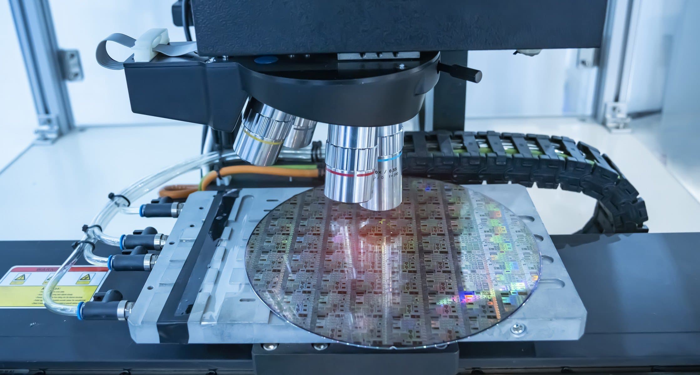
Metrology, physical inspection, and fabrication services
The exploration of next-generation semiconductor technologies – including advanced logic, memory and interconnect – necessitates a variety tools and techniques for metrology, physical inspection and fabrication.
It’s therefore one of the NanoIC pilot line’s goals to make sure innovators such as research centers, SMEs and high-level academia find a short and effortless path to Europe’s unique offering of advanced expertise in these domains.
This page provides an overview of services available at European research centers and universities that participate in the NanoIC project.
Metrology
Currently, you can access a wide variety of services at Tyndall and CSSNT.
Metrology services at Tyndall

Tyndall is one of Europe’s leading research institutes in microelectronics and photonics. It offers these metrology services:
- Scanning electron microscopy (SEM)
- Transmission electron microscopy (TEM), available 2026
- Energy-dispersive x-ray spectroscopy (EDX)
- Bright-field high-resolution transmission electrode spectroscopy (bright-field HRTEM), available in 2026
- Selected area electron diffraction analysis (SAED)
- High-angle annular dark-field imaging (HAADF)
- High-angle annular dark-field scanning transmission electron microscopy (HAADF-STEM), available in 2026
- Conductive atomic force microscopy (C-AFM)
- X-ray diffraction analysis (XRD)
- Raman spectroscopy
- X-ray photoelectron spectroscopy (XPS), available in 2026
These are located in three of Tyndall’s facilities/research programs:
Open Access Characterization
This state-of-the-art facility offers both wafer-level characterization of CMOS/MEMS test structures and precision measurement of impedance, capacitance, frequency spectrum, high voltage and high current.
CMOS++ Materials & Devices
This research program is geared to advancing future computing applications, such as quantum and neuromorphic, through innovative materials and devices.
For more information, send an email to Anthony Ginty, Research Translation Engineering Manager at Tyndall National Institute.
Precision Measurement Services at CSSNT

The Center for Surface Science and Nanotechnology (CSSNT), part of the National University of Science and Technology POLITEHNICA Bucharest (UPB), founded in 2011 by Professor Dr.rer.nat. Marius Enachescu, is a relatively young research facility, operating at the forefront of nanoscience and nanotechnology.
CSSNT houses 25 research and development laboratories, each of them centered on a piece of high-performance equipment or a group of equipment, with functionalities that satisfy the most demanding requirements of nanotechnology, but also many other related fields.
As of today, the Center offers multiple metrology services, in line with industry requirements, including:
- HR morphological properties studies via AFM (up to 300 mm)
- HR/UHR morphological properties studies via SEM (0.7 nm resolution) and STEM (0.14 nm resolution), obtaining three different image types at the same magnification in the same location, namely co-localized electron images through three different signal types: secondary electrons (SEM), incoherently scattered electrons (ZC – atomic number), and transmitted electrons (STEM)
- HR elemental analysis via EDX and EELS (TEM-correlated)
- FIB-based TEM lamella preparation
- Cryogenic transmission electron microscopy (cryo-TEM)
- Characterization of electrically active devices and/or structures via a nano-manipulators platform – HR-SEM, C-AFM, EFM/KPFM, SSRM, etc.
- Micro-/nano-mechanical properties investigation via PinPoint AFM, AFM-based micro-/nano-indenting, AFM-based micro-/nano-scratching
- Topography-correlated nanoscale IR-based chemical imaging (‘nano-FTIR’, sub-10nm spatial resolution), etc.
- Local strain detection at the nanoscale in IR-active materials (e.g. silicon oxide)
- Magnetic properties investigation via MFM
- Defects and/or contaminants detection and evaluation (e.g. SPM methods)
- Structural properties studies via HR-XRD
- Determination of chemical composition, nanostructure/phase, deformation/stresses by analyzing vibrational information from the chemical bond of a sample through micro-Raman spectroscopy
- Second Harmonic Generation (SHG) can be used to determine the crystal symmetry of a material, local polar order, domain structure, and interface properties by probing broken inversion symmetry in non-centrosymmetric materials
Click for more details about CSSNT’s infrastructure
Specific services offered by CSSNT as part of the NanoIC project are:
- FIB-based TEM lamellae processing
- (Cryo-)TEM-SEM-ZC-EDX/EELS characterization, acquiring co-localized images at the same magnification in the same location using three different image types: SEM, ZC, and STEM images
- AFM-IR: topography-correlated nano-IR chemical imaging and spectroscopy
- Cryo-focused ion eabm (Cryo-FIB)
- Second-harmonic generation (SHG)
Advanced electronic microscopy
By using high-resolution electron microscopy, these equipment help to provide analyses at both academic and industrial levels.
Atomic force microscopy - nano-infrared (AFM nano-IR)
AFM-IR enables the simultaneous imaging of sample topography and chemical properties (nano-IR imaging) with a spatial resolution below 10 nm. It also provides ‘nano-FTIR’ spectra by accurately measuring the near-field optical response of the sample through mechanical detection.
For more information, send an email to General Manager Prof. Dr.rer.nat. Marius Enachescu or the Assistant Project Coordinator Cristina Pavel.
Metrology services at VTT

VTT is a leading research, development, and innovation organisation in Europe. It contributes to the advancement and application of scientific and technological knowledge across commerce and society. VTT’s activities span multiple domains, including microelectronics and photonics.
Through NanoIC, VTT provides comprehensive metrology services for device and circuit characterization on 200 and 300 mm wafers, as well as for individual dies.
These services include:
- Semiconductor parameter analyzers for device measurements
- Network analyzers for S-parameter measurements up to 110 GHz
- Noise figure measurements up to 110 GHz
The measurements can be performed across a temperature range from –60 to +160°C and in most cases, also in cryogenic temperatures down to 20 K.
In addition to device and circuit characterization, VTT also offers circuit design services. Explore VTT’s full infrastructure and offering on the VTT website.
For more information, contact Tommi Suni, Customer Account Lead at VTT.
Physical inspection
Physical inspection services by Fraunhofer

- defect analysis on 3D packaged devices
- electrical fault localization
- lock-in thermography
- magnetic microscopy
- package-level physical failure analysis
- physical reliability testing
- virtual reliability assessment
These are located across these institutes:
Fraunhofer Institute for Microstructure of Materials and Systems (IMWS)
The IMWS specializes in materials science and materials engineering. You can contact them for issues connected to the microstructure of materials and systems: identifying defects and weak points, finding their causes and offer solutions.
Fraunhofer Institute for Electronic Nano Systems (ENAS)
The ENAS offers various test and reliablity solutions as part of its role as innovation partner in the field of smart systems.
Fraunhofer Institute for Reliability and Microintegration (IZM)
The collaborating departments within the IZM are on Wafer Level System Integration and System Integration & Interconnection Technologies.
For more information, send an email to Violeta Prodanovic.
Fabrication
You can access manufacturing services at Fraunhofer and Tyndall.
Fabrication services at Fraunhofer

The Fraunhofer Institute for Reliability and Microintegration (IZM) offers:
- single-chip bumping
- flip-chip assembly
- package balling
- device encapsulation (CUF, MUF, Molding)
- ADK generation
The collaborating departments within the IZM are on Wafer Level System Integration and System Integration & Interconnection Technologies.
For more information, send an email to Violeta Prodanovic.
Fabrication services at Tyndall

Tyndall offers 2D material deposition via ALD, through its CMOS++ Materials & Devices research program.
For more information, send an email to Anthony Ginty, Research Translation Engineering Manager at Tyndall National Institute.


